
Contents
- Contents
- VHDL
- Theory
- LUT
- Circuit technologies & FPGA configuration
- Clock and Synchronization
- Tidligere flervalgsoppgaver (Korrekte påstander)
- Høyhastighets serielinker
- Design
- FPGA-teknologi
- Klokkenet, DCM og design
- Metastabilitet og timing constraints
- Signalverdier i VHDL av typen std_logic:
- Konfigurasjon og lagringsteknologi
- VHDL og simulering
- Konfigurasjon og rekonfigurasjon av Xilinx FPGA
- Høyhastighets-linker
- Design og ASIC
- Konfigurasjon av FPGA
- Verktøy og metodikk
- DCM og klokkenett for Xilinx
- DSP konstruksjon
- Timing constraints for Xilinx
- En Xilinx FPGA kan inneholde harde kjerner for:
- Gigabit Transceivere
- Variabler i VHDL deklareres i:
- Kretsteknologier
- Lagringsteknologi
- Optimalisert FPGA design
- Prosessorkjerner
- Sykelbasert simulering
- Syntese
- SystemC
- Programmerings-teknologier for programmerbar logikk
- Størrelse på FPGA logikkblokker
- Klokkestyring
- (A)synkront design
- Verifikasjon
- Myke og harde prosessorkjerner
- Kodestil for FPGA og ASIC
- Valg mellom ASIC og FPGA
- Rekonfigurering av aktiv FPGA
VHDL
Package
A package is an optional library unit used for making shared definitions. An example of something that might be shared is a type definition, as shown in Figure 2-1. When you make definitions in a package, you must use the library and use statements to make the package available to other parts of the VHDL design.
package example_arithmetic is
	type small_int is range 0 to 7;
end example_arithmetic;

----------------------------------

package DEMO_PACK is
  constant SOME_FLAG : bit_vector := "11111111";
  type STATE is (RESET,IDLE,ACKA);
  component HALFADD
    port(A,B : in bit;
         SUM,CARRY : out bit);
  end component;
end DEMO_PACK;
Structure
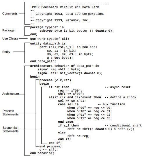
Entity
Entities contain the input and output definitions of the design. In VHDL designs that contain a hierarchy of lower-level circuits, the entity functions very much like a block symbol on a schematic.
library my_lib;
use my_lib.example_arithmetic.all;

entity ent is
	port (a0,a1,b0,b1 : in small_int; c0,c1 : out small_int);
end ent;
Architecture
The architecture is the actual description of the design. If you think of an entity as a functional block symbol on a schematic, then an architecture describes what’s inside the block. An architecture can contain both concurrent and sequential statements, which are described below. Note that VHDL allows you to have more than one architecture for the same entity. For example, you might have an architecture for synthesis and a gate-level (netlist) architecture. If you have more than one architecture for an entity, use configuration declarations to determine which architecture to use for synthesis or simulation. An architecture consists of two pieces: the architecture declaration section and the architecture body.
architecture behavioral of ent is
	signal c_internal: small_int;
begin
	c_internal <= a0 + b0;
	c0 <= c_internal;
	c1 <= c_internal + a1 + b1;
end behavioral;
Statements
Declaration Statements
Declaration statements are used to define constants (such as literal numbers or strings), types (such as records and arrays), objects (such as signals, variables and components), and subprograms (such as functions and procedures) that will be used in the design. Declarations can be made in many different locations within a VHDL design, depending on the desired scope of the item being declared.
Concurrent Statements
Concurrent statements define logic (typically in the form of signal assignments that include combinational logic) that is inherently parallel. With concurrent statements, values are carried on signals, which may be the actual input and output ports of the design (defined in an entity statement) or local signals declared using a signal declaration statement.
architecture dataflow of my_circuit is
	signal d,e bit;
begin
	-- concurrent statements tied together with signals
	d <= in3 and in4;
	-- logic for d
	e <= in5 or in6;
	-- logic for e
	out1 <= in1 xor d;
	-- output logic
	out2 <= in2 xor e;
	-- output logic
end dataflow;
Sequential Statements
Sequential statements are similar to statements used in software programming languages such as C or Pascal. The term sequential in VHDL refers to the fact that the statements execute in order, rather than to the type of logic generated. That is, you can use sequential statements to describe either combinational or sequential (registered) logic. With sequential statements, values may be carried using either signals or variables.
architecture behavior of some_thing is
begin
	process begin
		wait until clock;
		if (accelerator = '1') then
			case speed is
				when stop => speed <= slow;
				when slow => speed <= medium;
				when medium => speed <= fast;
				when fast => speed <= fast;
			end case;
		end if;
	end process;
end behavior;
Data Objects
Variables
Like a variable in C or Pascal, a variable in VHDL carries with it only one piece of information: its current value. Variables are assigned a value using the := operator. Consider the following variable assignments:
first_var := 45;
SECOND_VAR := first_var;
second_var := 0;
Before they can be used, variables must be declared with a variable declaration statement, as in the following example:
variable first_var : integer;
variable second_var, third_var : integer := 0;
Signals
Signals are declared in much the same manner as variables. Signal declarations may include an initial value, which will be ignored by the synthesis compiler. Examples of signal declarations are as follows:
signal first_sig : integer;
signal second_sig, third_sig : integer := 5;
Signal assignments are performed using the <= operator, as in the
following examples:
first_sig <= 9;
second_sig <= first_sig;
Data types
Std_logic
Std_ulogic (which is the base type of the more-commonly used resolved type std_logic) is a data type defined by IEEE standard 1164, and defined in the file ieee.vhd. Std_ulogic is an enumerated type, and has the following definition (from ieee.vhd):
type std_ulogic is (
'U',
-- Uninitialized
'X',
-- Forcing Unknown
'0',
-- Forcing 0
'1',
-- Forcing 1
'Z'
-- High Impedance
'W'
-- Weak Unknown
'L'
-- Weak 0
'H'
-- Weak 1
'-'
-- Don't care
);
Std_logic_vector
The std_logic_vector type is used for arrays of std_logic variables and signals.
The basic VHDL logic operations are defined on this type: and, nand, or, nor, xor, xnor. These must be given two arrays of the same size; they do the operation on ecah position and return another array. The not operation negates each position in the array.
signal s1, s2, s3 : std_logic_vector(3 downto 0);
...
s1(0) <= '0';
s1(1) <= '1';
s1(2) <= '1';
s1(3) <= '0';
s2 <= "1100";     -- sets s(3),s(2) to '1', s(1),s(0) to '0': same order as range in declaration
s3 <= s2          -- copies all of s2 into s3
s3 <= s1 and s2;  -- "0100"
Type Conversions
Any given VHDL FPGA design may have multiple VHDL types being used. The most common VHDL types used in synthesizable VHDL code are std_logic, std_logic_vector, signed, unsigned, and integer. Because VHDL is a strongly-typed language, most often differing types cannot be used in the same expression. In cases where you can directly combine two types into one expression, you are really leaving it up to the compiler or synthesis tool to determine how the expression should behave, which is a dangerous thing to do.
signal slv : std_logic_vector(7 downto 0);
signal s : signed(7 downto 0);
signal us : unsigned(7 downto 0);
--FROM std_logic_vector TO signed/unsigned
sgn <= signed(slv);
usgn <= unsigned(slv);
-- FROM signed/unsigned TO std_logic_vector
svl <= std_logic_vector(sgn);
svl <= std_logic_vector(usgn);
Operators
**exponentiation, numeric ** integer, result numericabsabsolute value, abs numeric, result numeric-
notcomplement, not logic or boolean, result same *multiplication, numeric * numeric, result numeric/division, numeric / numeric, result numericmodmodulo, integer mod integer, result integer-
remremainder, integer rem integer, result integer +unary plus, + numeric, result numeric-
-unary minus, - numeric, result numeric +addition, numeric + numeric, result numeric-subtraction, numeric - numeric, result numeric-
&concatenation, array or element & array or element, result array sllshift left logical, logical array sll integer, result samesrlshift right logical, logical array srl integer, result sameslashift left arithmetic, logical array sla integer, result samesrashift right arithmetic, logical array sra integer, result samerolrotate left, logical array rol integer, result same-
rorrotate right, logical array ror integer, result same =test for equality, result is boolean/=test for inequality, result is boolean<test for less than, result is boolean<=test for less than or equal, result is boolean>test for greater than, result is boolean-
>=test for greater than or equal, result is boolean andlogical and, logical array or boolean, result is sameorlogical or, logical array or boolean, result is samenandlogical complement of and, logical array or boolean, result is samenorlogical complement of or, logical array or boolean, result is samexorlogical exclusive or, logical array or boolean, result is samexnorlogical complement of exclusive or, logical array or boolean, result is same
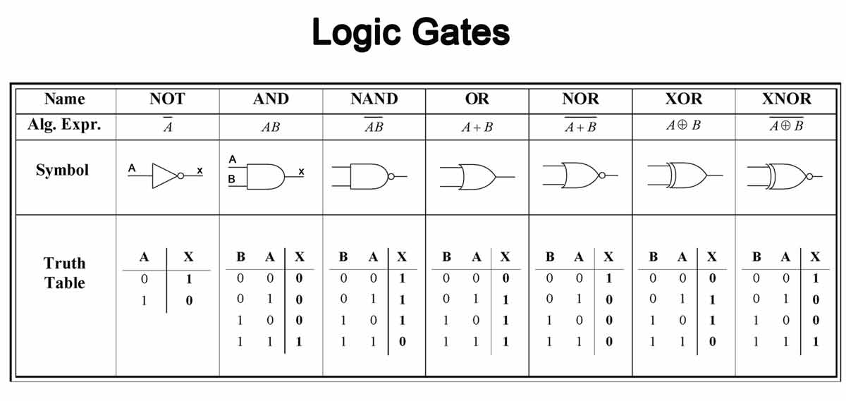
Combinatorial logic
Logical Operators
entity logical_ops_1 is
	port (a, b, c, d: in bit; m: out bit);
end logical_ops_1;

architecture example of logical_ops_1 is
	signal e: bit;
begin
	m <= (a and b) or e; --concurrent signal assignments
	e <= c xor d;
end example;

-------------------------------------------------------

entity logical_ops_2 is
	port (a, b: in bit_vector (0 to 3);
		m: out bit_vector (0 to 3));
end logical_ops_2;

architecture example of logical_ops_2 is
begin
	m <= a and b;
end example;
Relational Operators
entity relational_ops_1 is
	port (a, b: in bit_vector (0 to 3); m: out Boolean);
end relational_ops_1;

architecture example of relational_ops_1 is
begin
	m <= a = b;
end example;

----------------------------------------------------

entity relational_ops_2 is
	port (a, b: in integer range 0 to 3; m: out Boolean);
end relational_ops_2;

architecture example of relational_ops_2 is
begin
	m <= a >= b;
end example;
Arithmetic Operators
package example_arithmetic is
	type small_int is range 0 to 7;
end example_arithmetic;

use work.example_arithmetic.all;

entity arithmetic is
	port (a, b: in small_int; c: out small_int);
end arithmetic;

architecture example of arithmetic is
begin
	c <= a + b;
end example;
Conditional Logic
Conditional Signal Assignment
entity control_stmts is
	port (a, b, c: in Boolean; m: out Boolean);
end control_stmts;

architecture example of control_stmts is
begin
	m <= b when a else c;
end example;
Selected Signal Assignment
library ieee;
use ieee.std_logic_1164.all;

entity ex_select is
end ex_select;

architecture behave of ex_select is

  signal r_Index   : integer := 2;
  signal w_One_Hot : std_logic_vector(3 downto 0);

begin

  with r_Index select
    w_One_Hot <= "0000" when 0,
                 "0001" when 1,
                 "0010" when 2,
                 "0100" when 3,
                 "1000" when 4,
                 "0000" when others;

end behave;
If Statement
library ieee;
use ieee.std_logic_1164.all;
use ieee.numeric_std.all;

entity example_if_statement is
  generic (
    g_INIT : natural := 1        -- 0="DEAD", 1="BEEF"
    );
end example_if_statement;

architecture behave of example_if_statement is

  signal r_CHOICE : std_logic_vector(1 downto 0)  := "00";
  signal r_VECTOR : std_logic_vector(15 downto 0) := (others => '0');

begin

  -- If statement outside of a process (requires generate keyword)
  g_IF_SETTING_1 : if g_INIT = 0 generate
    r_VECTOR <= X"DEAD";
  end generate g_IF_SETTING_1;

  g_IF_SETTING_2 : if g_INIT = 1 generate
    r_VECTOR <= X"BEEF";
  end generate g_IF_SETTING_2;


  -- If statement inside of a process
  p_IF_TEST : process (r_VECTOR) is
  begin
    if r_VECTOR = X"DEAD" then
      r_CHOICE <= "01";
    elsif r_VECTOR = X"BEEF" then
      r_CHOICE <= "10";
    else
      r_CHOICE <= "11";
    end if;
  end process p_IF_TEST;

end behave;
Case Statement
library ieee;
use ieee.std_logic_1164.all;

entity example_case_statement is
end example_case_statement;

architecture behave of example_case_statement is

  signal r_VAL_1  : std_logic := '0';
  signal r_VAL_2  : std_logic := '0';
  signal r_VAL_3  : std_logic := '0';
  signal r_RESULT : integer range 0 to 10;

begin


  -- Uses r_VAL_1, r_VAL_2, and r_VAL_3 together to drive a case statement
  -- This process is synthesizable
  p_CASE : process (r_VAL_1, r_VAL_2, r_VAL_3)
    variable v_CONCATENATE : std_logic_vector(2 downto 0);
  begin
    v_CONCATENATE := r_VAL_1 & r_VAL_2 & r_VAL_3;

    case v_CONCATENATE is
      when "000" | "100" =>
        r_RESULT <= 0;
      when "001" =>
        r_RESULT <= 1;
      when "010" =>
        r_RESULT <= 2;
      when others =>
        r_RESULT <= 9;
    end case;

  end process;


  -- This process is NOT synthesizable.  Test code only!
  -- Provides inputs to code and prints debug statements to console.
  p_TEST_BENCH : process is
  begin
    r_VAL_1 <= '0';
    r_VAL_2 <= '0';
    r_VAL_3 <= '0';
    wait for 100 ns;
    r_VAL_2 <= '0';
    r_VAL_3 <= '1';
    wait for 100 ns;
    r_VAL_2 <= '1';
    r_VAL_3 <= '0';
    wait for 100 ns;
    r_VAL_2 <= '1';
    r_VAL_3 <= '1';
    wait for 100 ns;
    wait;
  end process;

end behave;
Replicated Logic
Functions and Procedures
library ieee;
use ieee.std_logic_1164.all;
use ieee.numeric_std.all;

entity example_function_advanced is
end example_function_advanced;

architecture behave of example_function_advanced is

  signal r_TEST_ASCII : std_logic_vector(7 downto 0) := X"42";
  signal r_TEST_HEX   : std_logic_vector(3 downto 0) := (others => '0');

  -- Purpose: This function converts ascii characters to hexadecimal.
  -- Numbers are 0x30-0x39 so only interpret least sig nibble.
  function f_ASCII_2_HEX (
    r_ASCII_IN : in std_logic_vector(7 downto 0))
    return std_logic_vector is
    variable v_TEMP : std_logic_vector(3 downto 0);
  begin
    if (r_ASCII_IN = X"41" or r_ASCII_IN = X"61") then
      v_TEMP := X"A";
    elsif (r_ASCII_IN = X"42" or r_ASCII_IN = X"62") then
      v_TEMP := X"B";
    elsif (r_ASCII_IN = X"43" or r_ASCII_IN = X"63") then
      v_TEMP := X"C";
    elsif (r_ASCII_IN = X"44" or r_ASCII_IN = X"64") then
      v_TEMP := X"D";
    elsif (r_ASCII_IN = X"45" or r_ASCII_IN = X"65") then
      v_TEMP := X"E";
    elsif (r_ASCII_IN = X"46" or r_ASCII_IN = X"66") then
      v_TEMP := X"F";
    else
      v_TEMP := r_ASCII_IN(3 downto 0);
    end if;
    return std_logic_vector(v_TEMP);
  end;

  -- Purpose: This function performs a bitwise xor on the input vector
  function f_BITWISE_XOR (
    r_SLV_IN    : in std_logic_vector)
    return std_logic is
    variable v_XOR : std_logic := '0';
  begin
    for i in 0 to r_SLV_IN'length-1 loop
      v_XOR := v_XOR xor r_SLV_IN(i);
    end loop;
    return v_XOR;

  end function f_BITWISE_XOR;


begin

  process is
  begin
    r_TEST_HEX   <= f_ASCII_2_HEX(r_TEST_ASCII);  -- function

    if f_BITWISE_XOR(r_TEST_ASCII) = '1' then
      report "RX Character has Odd Parity" severity note;
    else
      report "RX Character has Even Parity" severity note;
    end if;

    wait for 10 ns;

    r_TEST_ASCII <= X"37";
    wait for 10 ns;
    r_TEST_HEX   <= f_ASCII_2_HEX(r_TEST_ASCII);  -- function

    if f_BITWISE_XOR(r_TEST_ASCII) = '1' then
      report "RX Character has Odd Parity" severity note;
    else
      report "RX Character has Even Parity" severity note;
    end if;

    wait;
  end process;

end behave;

----------------------------------------------------------------------

library ieee;
use ieee.std_logic_1164.all;
use ieee.numeric_std.all;

entity example_procedure_simple is
end example_procedure_simple;

architecture behave of ex_procedure_simple is

  signal r_TEST : std_logic_vector(7 downto 0) := X"42";

  -- Purpose: Increments a std_logic_vector by 1
  procedure p_INCREMENT_SLV (
    signal r_IN  : in  std_logic_vector(7 downto 0);
    signal r_OUT : out std_logic_vector(7 downto 0)
    ) is
  begin
    r_OUT <= std_logic_vector(unsigned(r_IN) + 1);
    wait for 1 ns;                      -- Wait is OK here.
  end p_INCREMENT_SLV;


begin

  process is
  begin
    wait for 10 ns;
    p_INCREMENT_SLV(r_TEST, r_TEST);
    wait for 10 ns;
    p_INCREMENT_SLV(r_TEST, r_TEST);
    wait for 10 ns;
    p_INCREMENT_SLV(r_TEST, r_TEST);
    wait;
  end process;

end behave;
Loop Statements
entity loop_stmt is
	port (a: in bit_vector (0 to 3);
		m: out bit_vector (0 to 3));
end loop_stmt;

architecture example of loop_stmt is
begin
	process (a)
		variable b:bit;
	begin
		b := 1;
		for i in 0 to 3 loop -- no need to declare i
			b := a(3-i) and b;
			m(i) <= b;
		end loop;
	end process;
end example;

-----------------------------------------------------

entity while_stmt is
	port (a: in bit_vector (0 to 3);
		m: out bit_vector (0 to 3));
end while_stmt;

architecture example of while_stmt is
begin
process (a)
variable b: bit;
variable i: integer;
begin
	i := 0;
		while i < 4 loop
			b := a(3-i) and b;
			m(i) <= b;
		end loop;
	end process;
end example;
Finite State Machines
library ieee;
use ieee.std_logic_1164.all;
entity machine is
	port (clk,reset: in std_logic;
		state_inputs: in std_logic_vector (0 to 1);
		comb_outputs: out std_logic_vector (0 to 1));
end machine;

architecture behavior of machine is
	type states is (st0, st1, st2, st3);
	signal present_state, next_state: states;
begin
	register: process (reset,clk)
	begin
		if reset = '1' then
			present_state <= st0; -- async reset to st0
		elsif rising_edge(clk) then
			present_state <= next_state; -- transition on clock
		end if;
	end process;

	transitions: process(present_state, state_inputs)
	begin
		case current_state is -- describe transitions
			when st0 =>
				-- and comb. outputs
				comb_outputs <= "00";
				if state_inputs = "11" then
					next_state <= st0;
					-- hold
				else
					next_state <= st1;
					-- next state
				end if;
			when st1 =>
				comb_outputs <= "01";
				if state_inputs = "11" then
					next_state <= st1;
					-- hold
				else
					next_state <= st2;
					-- next state
				end if;
			when st2 =>
				comb_outputs <= "10";
				if state_inputs = "11" then
					next_state <= st2;
					-- hold
				else
					next_state <= st3;
					-- next state
				end if;
			when st3 =>
				comb_outputs <= "11";
				if state_inputs = "11" then
					next_state <= st3;
					-- hold
				else
					next_state <= st0;
					-- next state
			end if;
		end case;
	end process;
end behavior;
Moore machine
In a Moore machine, the output is a function of the current state only, and can change only on a clock edge. In the following architecture, F1 and F2 are combinational logic functions of an arbitrary complexity. A simple state machine implementation maps each block to a VHDL process:
library ieee;
use ieee.std_logic_1164.all;

entity system is
	port (clock: in std_logic;
	A: in std_logic;
	D: out std_logic);
end system;

architecture moore1 of system is
signal B, C: std_logic;
begin
	F1: process (A, C)
	-- Next state logic
	begin
		B <= F1(A, C);
	end process;

	F2: process (C)
	-- Output logic
	begin
		D <= F2(C);
	end process;

	Register: process (clock) -- State registers
	begin
		if rising_edge(clock) then
			C <= B;
		end if;
	end process;
end moore1;
Mealy machine
A Mealy machine always requires two processes (or one process for the machine and separate concurrent statements for the outputs,) as its timing is a function of both the clock and the data inputs:
architecture mealy of system is
	signal C: std_logic;
begin
	Combinational: process (A,C) -- Mealy outputs
	begin
		D <= F2(A, C);
	end process;

	Registers: process (clock)
	-- State machine logic
	begin
		if rising_edge(clock) then
			C <= F1(A, C);
		end if;
	end process;
end mealy;
Avoiding Unwanted Latches
When describing state machines in VHDL, you must be careful to avoid the creation of unwanted asynchronous feedback paths that form latches. The rules of VHDL state that a signal within a process whose value is not completely specified (provided with an explicit assignment for all possible input conditions) will hold its previous value for the unspecified conditions. Latches can therefore be inadvertently created by incompletely specifying the transitions from one or more states in a state machine, or by failing to specify the value of all outputs in the states of the machine.
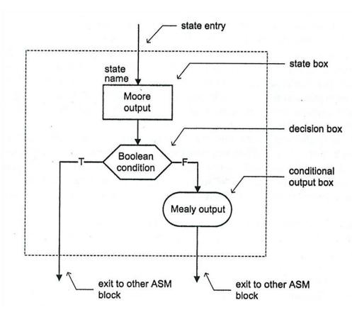
ASM Diagrams
-
The state box represents the state in the FSM, and the output in the state box describes the desired output values when the FMS enters this state (i.e. the Moore outputs).
-
The decision box tests an input condition to determine the exit path of the current ASM block.
-
A conditional output box also lists asserted signals. It can only be placed after a exit path of a decision box (i.e. the Mealy outputs that depends on the state and the input values).
-
Note that the conditional output box can only be placed after an exit path of a decision box.
-
<=is used for assigning signal values. -
Use
<-for register operations!
Holy rules:
- For a given input combination, there is one unique exit path from the current ASM block.
- The exit path of an ASM block must always lead to a state box. The state box can be the state box of the current ASM block or of another ASM block.
Register use:
- Register is updated when the FSM exits current state
- Use the solution on the right side!
Test beches
Simple testbench
library IEEE;
use IEEE.Std_Logic_1164.all;

entity TEST_FIRST is
  -- The entity for a testbench is normally empty
end TEST_FIRST;

architecture TESTBENCH of TEST_FIRST is

  -- Component declarations
  Component FIRST
    port
    (
      CLK        : in  std_logic; -- Clock from switch CLK1/INP1
      RESET      : in  std_logic; -- Global Asynchronous Reset
      LOAD       : in  std_logic; -- Synchronous Reset
      INP        : in  std_logic_vector(3 downto 0); -- Start Value
      COUNT      : out std_logic_vector(3 downto 0); -- Counting value
      MAX_COUNT  : out std_logic  -- Max counting value
    );
  end Component;

  --testbench internal signals
  --which should be used to connect with the component first
  --input to UUT should be given initial values
  signal  MCLK        : std_logic := '0'; --:= initial value
  signal  RESET      : std_logic := '0';
  signal  LOAD       : std_logic := '0';
  signal  INP        : std_logic_vector(3 downto 0) := "0000";
  signal  COUNT      : std_logic_vector(3 downto 0);
  signal  MAX_COUNT  : std_logic;

  constant Half_Period : time := 10 ns;  --50Mhz klokkefrekvens

begin

  --Instantiates "Unit Under Test", UUT
  UUT : FIRST
  port map
  (
  --<formal name> => <actual name>
    CLK        =>  MCLK,
    RESET      =>  RESET,
    LOAD       =>  LOAD,
    INP        =>  INP,
    COUNT      =>  COUNT,
    MAX_COUNT  =>  MAX_COUNT
  );

  -- Defines the clock
  MCLK <= not MCLK after Half_Period;

  -- The input stimuli to UUT
  STIMULI :
  process
  --a process with an empty sensitivity list should include wait statements
  begin
    RESET <= '1', '0' after 100 ns;
    INP <= "1010" after Half_Period*6;
    wait for 2*Half_Period*10;
    LOAD <= '1', '0' after 2*Half_Period;
    --wait;
  end process;

end TESTBENCH;
Finite state machine testbench
library IEEE;
use IEEE.std_logic_1164.all;

entity T_TRAFFICCTRL is
end entity T_TRAFFICCTRL;

architecture TEST_TRAFFICCTRL of T_TRAFFICCTRL is

  component TRAFFICCTRL is
    port
      (
        CLOCK       : in  std_logic;
        RESET       : in  std_logic;
        CAR         : in  std_logic;
        MAJOR_GREEN : out std_logic;
        MINOR_GREEN : out std_logic
        );
  end component trafficctrl;


  signal CLOCK       : std_logic := '0';
  signal RESET       : std_logic := '1';
  signal CAR         : std_logic := '0';
  signal MAJOR_GREEN : std_logic;
  signal MINOR_GREEN : std_logic;

begin

  TRAFFICCTRL_INST : TRAFFICCTRL
    port map
    (
      CLOCK       => CLOCK,
      RESET       => RESET,
      CAR         => CAR,
      MAJOR_GREEN => MAJOR_GREEN,
      MINOR_GREEN => MINOR_GREEN
      );

  CLOCK <= not CLOCK after 10 ns;

  STIMULI :
  process
  begin
    RESET <= '1', '0' after 100 ns;
    wait for 1 us;
    CAR   <= '1';
    wait for 200 ns;
    CAR   <= '0';
    wait;
  end process;

end architecture TEST_TRAFFICCTRL;
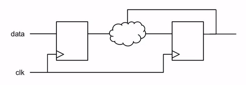
Synchronize signals
s1 and s2 are external
architecture beh of sync_ex is

signal tmp_s1 : signed (7 downto 0 ) ;
signal tmp_s2 : signed (7 downto 0 ) ;
signal syncd_s1 : signed (7 downto 0 ) ;
signal syncd_s2 : signed (7 downto 0 ) ;

begin
sync :
	process (clk)
	begin
		if (rising_edge(clk)) then
			tmp_s1 <= s1 ;
			tmp_s2 <= s2 ;
			syncd_s1 <= tmp_s1 ;
			syncd_s2 <= tmp_s2 ;
		end if;
	end process sync;
end architecture beh;
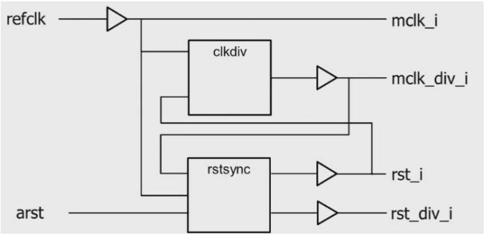
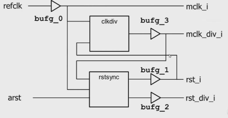
CRU
- Collects gates associated with clock and reset in one place
- Makes it easy to review
- How clocks are generated
- That clock and reset are handled correctly
- Placed at the top level of your design
Example presented:
- Divides clock by 128
- Synchronizes reset to both clock domains
Clk div
library ieee;
use ieee.std_logic_1164.all;

entity clkdiv is
  port (
    rst       : in  std_logic;
    mclk      : in  std_logic;
    mclk_div  : out  std_logic
    );
end clkdiv;

----------------------------------------

library ieee;
use ieee.std_logic_1164.all;
use ieee.numeric_std.all;

architecture rtl of clkdiv is
  signal mclk_cnt : unsigned(8 downto 0);
begin

  P_CLKDIV: process(rst, mclk)
  begin
    if rst = '1' then
      mclk_cnt <= (others => '0');
    elsif rising_edge(mclk) then
      mclk_cnt <= mclk_cnt + 1;
    end if;
  end process P_CLKDIV;

  mclk_div <= std_logic(mclk_cnt(8));

end rtl;
Sync reset
library ieee;
use ieee.std_logic_1164.all;

entity rstsync is
  port (
    arst       	: in  std_logic;
    mclk      	: in  std_logic;
    mclk_div  	: in  std_logic;
    rst 		: out std_logic;
	rst_div		: out std_logic
	);
end rstsync;

----------------------------------

library ieee;
use ieee.std_logic_1164.all;
use work.all;

architecture rtl of rstsync is

  signal rst_s1, rst_s2 : std_logic;
  signal rst_div_s1, rst_div_s2 : std_logic;

begin

  P_RST_0 : process(arst, mclk)
  begin
    if arst = '1' then
      rst_s1 <= '1';
      rst_s2 <= '1';
    elsif rising_edge(mclk) then
      rst_s1 <= '0';
      rst_s2 <= rst_s1;
    end if;
  end process P_RST_0;

  P_RST_1 : process(arst, mclk_div)
  begin
    if arst = '1' then
      rst_div_s1 <= '1';
      rst_div_s2 <= '1';
    elsif rising_edge(mclk_div) then
      rst_div_s1 <= '0';
      rst_div_s2 <= rst_div_s1;
    end if;
  end process P_RST_1;

  rst <= rst_s2;
  rst_div <= rst_div_s2;

end rtl;
CRU
library ieee;
use ieee.std_logic_1164.all;

entity cru is
  port (
    arst      : in  std_logic;
    refclk    : in  std_logic;
    rst       : out  std_logic;
    rst_div   : out  std_logic;
    mclk      : out  std_logic;
    mclk_div  : out  std_logic
    );
end cru;

-------------------------------
library ieee;

use ieee.std_logic_1164.all;
library unisim;
use unisim.all;

architecture str of cru is

  component bufg
    port (i : in std_logic;
          o : out std_logic);
  end component;

  component rstsync is
    port (arst    : in std_logic;
          mclk    : in std_logic;
          mclk_div: in std_logic;
          rst     : out std_logic;
          rst_div : out std_logic);
  end component rstsync;

  component clkdiv is
    port(rst      : in std_logic;
         mclk     : in std_logic;
         mclk_div : out std_logic);
  end component clkdiv;

  signal rst_i          : std_logic;
  signal rst_local      : std_logic;
  signal rst_div_local  : std_logic;
  signal rst_div_i      : std_logic;
  signal mclk_i         : std_logic;
  signal mclk_div_local : std_logic;
  signal mclk_div_i     : std_logic;

  begin

    bufg_0: bufg
      port map (
        i         => refclk,
        o         => mclk_i);

    rstsync_0: rstsync
      port map (
        arst      => arst,
        mclk      => mclk_i,
        mclk_div  => mclk_div_i,
        rst       => rst_local,
        rst_div   => rst_div_local);

    bufg_1: bufg
      port map (
        i         => rst_local,
        o         => rst_i);

	bufg_2: bufg
      port map (
        i         => rst_div_local,
        o         => rst_div_i);

    clkdiv_0: clkdiv
      port map (
        rst       => rst_i,
        mclk      => mclk_i,
        mclk_div  => mclk_div_local);


    bufg_3: bufg
      port map (
        i         => mclk_div_local,
        o         => mclk_div_i);

    rst       <= rst_i;
    rst_div   <= rst_div_i;
    mclk      <= mclk_i;
    mclk_div  <= mclk_div_i;

end str;
Theory
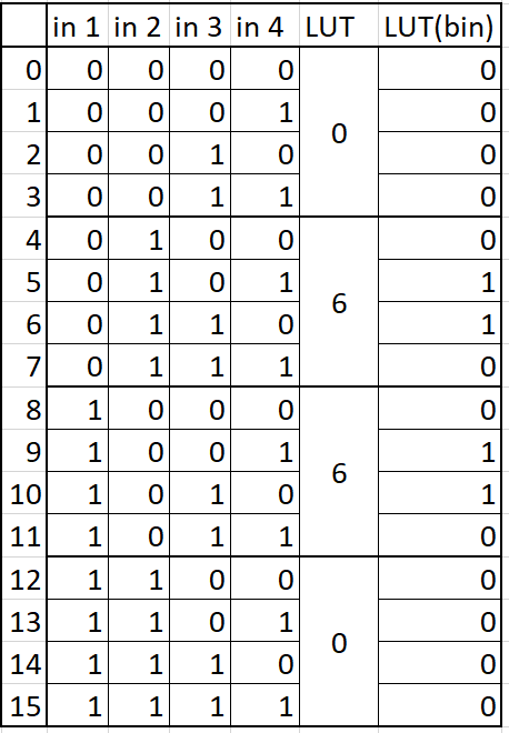
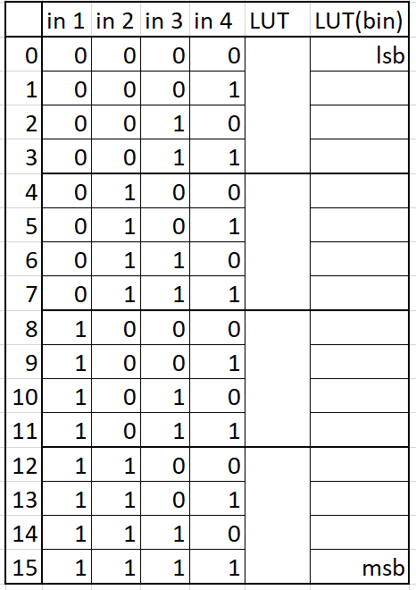
LUT
Look-up tables are how your logic actually gets implemented. A LUT consits of some number of inputs and one output. What makes a LUT powerful is that you can program what the output should be for every single possible input.
A LUT consists of a block of RAM that is indexed by the LUT’s inputs. The output of the LUT is whatever value is in the indexed location in it’s RAM.
Example of 4-input Xilinx LUT with (INITSTAT) “0660” (hex) contents:
| Tables | Logic circuits |
|---|---|
 |
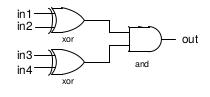 |
Table template
Circuit technologies & FPGA configuration
Basic overview of programmable logic devices
Notes and abbreviations
Programmable logic device (PLD):
- Simple Programmable Logic Device (SPLD)
- Complex Programmable Logic Devices (CPLD)
- Field Programmable Gate Array (FPGA)
Not re-programmale logic circuits :
- Application-Specific Standard Parts (ASSPs)
- Application Specific Integrated Circuit (ASICs) System On Chip (SoC)
Random-Access Memory (RAM)
- Stores binary information on groups of bits.
- RAM is volatile, information stored disappears when powered off.
- Static RAM uses flip-flops to store, while Dynamic RAM uses electronic charges on capacitors.
Programmable Read Only Memory (ROM)
- Similar to RAM, different storage technology.
- 1 decoder (\(n\) inputs and \(2^n\) outputs) + m OR gates.
- Not reprogrammable
Programmable Logic Array (PLA)
- Programmable AND-array and fixed OR-array.
- Can not share AND terms between different OR-terms.
- Re-programmable devices exist(GAL).
Families of PLDs
SPLD - Simple Programmable Logic Device
- Smallest and cheapest
- Programming:
- Fuses or non-volatile memory; EPROM, EEPROM or FLASH.
CPLD - Complex Programmable Logic Device
- From 2 to 64 times more logic than SPLD.
- Same programming as SPLD
FPGA - Field Programmable Gate Array
- Much more logic than CPLD.
- Programming:
- Static memory(SRAM) or anti-fuse technology.
- Some exist with EEPROM or FLASH.
FPGA vs CPLD
- Use CPLD when:
- Simple or time critical designs
- Large volume products
- Mobile and low power applications
- FPGA is first choice other than the mentioned above.
ASIC
- IC customized for particular use.
- Not re-programmable
- Examples:
- High-efficiency Bitcoin miner
FPGA, architecture and configuration
Antifuse-based
- Config is saved in the FPGA via shorts using high voltage.
- Advantages:
- Low impedance = small delay (When fuse is on).
- Low power usage
- Compact
- High radiation resistance
- Disadvantages:
- Needs dedicated programmer
- High programming voltage and power
- One-time programming
SRAM-based
- SRAM saves config
- Advantages:
- Re-programmable
- More logic
- Easy functionality changes
- No need for dedicated programmer or process
- Disadvantages:
- More space required
- Volatile memory
- High power usage
Fine grained complexity
- Less logic per block
- Requires large routeing resources
- This gives more delay
Coarse grained complexity
- More logic
- Can implement any arbitrary function, but the resources can often no be fully exploited
- Complexity increases with technological progress
- Example:
- Four 4-input LUT
- Four multiplexers
- 4 D-flip flops
- Carry logic for efficient arithmetic
Additional functions in modern FPGAs
- RAM blocks
- Often used for FIFO functions, state machines etc.
- Function blocks
- Multipliers
- Adders
- Multiply-and-accumulate (MAC)
- Processor cores
- Soft core
- Implemented by the logic blocks
- Slower than Hard cores
- Can implement as many cores as you want and when you need it
- Hard core
- Dedicated cores on the same fabric
- Faster than soft cores
- Static
- Soft core
- Clock generation and distribution
- Distribute clock signals to synchronous elements across the device
- Generates a number of derived clocks from the global clock
Clock and Synchronization
Timing of a combinatorial digital system
- Steady state
- Signal reaches a stable value
- Modeled by Boolean algebra
- Transient period
- Signal may fluctuate
- No simple model
- Propagation delay: time to reach the steady state
Timing hazards
- Hazards: the fluctuation occurring during the transient period
- Static hazard: glitch when the signal should be stable
- Dynamic hazard: a glitch in transition
- Du to several converging paths of an output
How to properly handle them
- Ignore glitches in the transient period and retrieve the data after signal is stabilized
- Utilize a clock signal to sample the signal and store the stable value in a register.
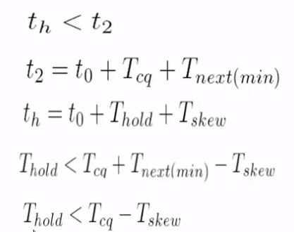
- NB! Registers introduces constraint (setup and hold time)
Synchronous system
- group registers and drive them with the same clock
Clock skew
- time difference between two arriving clock edges
Setup time
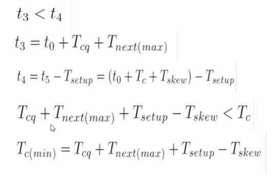
Hold time
- Has to be fixed during physical synthesis
Summary:
- Clock skew normally has negative impact on synchronous sequential circuit
- Effect on setup time constraint: require to increase clock period(reduce clock rate)
- Effect on hold time constraint: may introduce hold time violation
Multiple clock systems
- Necessary due to:
- multiple clock sources
- design complexity
- circuit size
- power consideration
GALS
- Globally asynchronous locally synchronous system
Meta-stability and synchronization failure
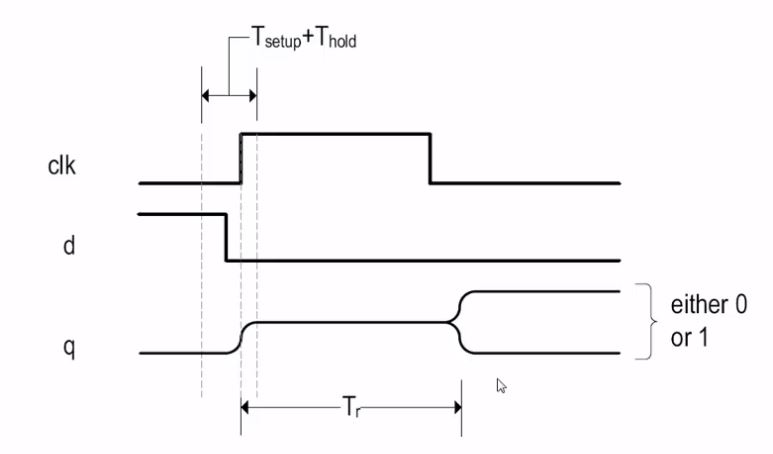
- FF eventually “resolves” to one of stable states
- The probability that metastability persist beyond Tr
- \[P(T-r)=e^{-\frac{T_r}{\tau}}\]
Synchronization circuits
- No physical circuit can prevent metastability
- Synchronization just provides enough time for the metastable condition to be resoled
Notes on synchronization
- Metastability cannot easily be modeled or simulated in gate level
- Metastability cannot be easily observed or measured in physical circuit
- When done wrong, MTBF is very sensitive to circuit revision
Enable pulse crossing clock domain
- Synchronizer just ensures that the receiving system does not enter a metastable state
- It does not guarantee the function of the received signal
Tidligere flervalgsoppgaver (Korrekte påstander)
Høyhastighets serielinker
- Differensielle signaler brukes for å redusere støy problemer.
- 8B/10B signal koding brukes for å unngå flere enn 8 påfølgende like bit.
- For PCIe gen. 1 er faktisk datarate 2.0 Gbit/s med 8B/10B koding som gjør at linjens baudrate blir 2.5 Gbit/s. \(\frac{2.5}{10} * 8 = 2.0\)
- Grunnen til at en overført firkantpuls ved høy datarate kan bli lik et sinussignal er at høyfrekvent frekvensinnhold har blitt kraftig dempet
- Konfigurasjon av parametere i transceiver muliggjør design med forskjellige kommunikasjonsstandarder
- Pre-emphasis motvirker dempning i overført signal
Design
- Med en Digital Clock Manager (DCM) modul kan man øke klokkesignalet til det firedobbelte og det genererte klokkesignalet vil være i fase med inngangsklokken.
- I en Xilinx FPGA har set inngangen til en flip-flop lavere prioritet enn reset inngangen.
- En Xilinx Block RAM har to uavhengige porter som begge kan leses fra og skrives til samtidig.
- Tilbakekoblingssløyfer med flip-flop’er kan brukes i en FPGA. Asynkront design anbefales ikke i en FPGA.
- Integrering av et helt system med prosessor på en krets gir en mer kompakt løsning som prismessig kan være gunstig.
- En hard prosessorkjerne er vanligvis raskere (høyere klokkefrekvens) enn en myk prosessorkjerne.
- RAM kan lages av LUT’er.
- En Xilinx Block RAM har to uavhengige porter som begge kan leses fra og skrives til samtidig.
- Det er begrenset hvor mange adskilte klokkerlinjer fra BUFG’er som finnes i en FPGA i forhold til i en ASIC.
- Med en Digital Clock Manager modul kan man øke klokkesignalet til det dobbelt og det genererte signalet kan være i fase med inngangsklokken.
- En hard prosessorkjerne tar vanligvis mindre plass enn en myk prosessorkjerne.
- I et klokkedomene klokkes alle registre (flipflop’er) med samme klokkesignal.
- I serielle linker har 8B/10B encoding mindre overhead enn 64B/66B enkoding.
- Intellectual Property (IP) er i FPGA teknologi en betegnelse på myke ferdigutviklede moduler.
- En hard IP kjerne tar mindre plass enn en tilsvarende myk IP kjerne.
- En Flash FPGA er umiddelbart aktiv etter strømtilkobling.
- Det må vanligvis brukes registere (flip-flop’er) i en tilbakekobling i FPGA.
- I en Xilinx FPGA har set inngangen til en flipflop/register lavere prioritet enn reset inngangen.
- En Xilinx Block RAM har to uavhengige porter som begge kan leses fra og skrives til.
FPGA-teknologi
- Forbindelseslinjer mellom LUT’er har vanligvis større tidsforsinkelse enn tidsforsinkelsen gjennom LUT’er i SRAM-teknologi.
- En FPGA krets basert på Flash er umiddelbart aktiv etter strømtilkobling.
- JTAG porten kan brukes både til konfigurasjon og til debugging.Block RAM’er har en kjent initialverdi etter konfigurering.
- En FPGA i master-modus styrer selv nedlastning av konfigurasjonen ved oppstart.
Klokkenet, DCM og design
- DCM kan forsinke en generert klokke slik at den er i fase med inngangsklokken.Antall nivåer med logikk i en FPGA mellom klokkede flipflop’er/registere har betydning for maksimal klokkefrekvensen.
- FPGA egner seg for pipelining pga. mange registere.
Metastabilitet og timing constraints
- Det er ikke enkelt å oppdage metastabilitet ved simulering.
- Deaktivering av et eksternt reset signal må alltid synkroniseres for alle klokkedomener hvor reset brukes.
Signalverdier i VHDL av typen std_logic:
- To signaler av typen std_logic med verdiene ’0’ og ’0’ som driver samme signal får verdien ’0’.
- To signaler av typen std_logic med verdiene ’0’ og ’1’ som driver samme signal får verdien ’X’.
Konfigurasjon og lagringsteknologi
- JTAG porten kan brukes både til konfigurasjon og til debugging.
- En FPGA i master-modus styrer selv nedlasting av konfigurasjon ved oppstart.
- Antifuse FPGA’er kan bare konfigureres en gang.
VHDL og simulering
- Det er raskere og enklere å simulere med variabler enn med signaler i en process.
- Alle variabler som er deklarert i en process vil ikke bli satt tilbake til sin initialverdi neste gang processen utføres.
Konfigurasjon og rekonfigurasjon av Xilinx FPGA
- Et problem ved dynamisk rekonfigurering er vanligvis for lang rekonfigureringstid.
- En mikroprocessor kan konfigurere en FPGA som er i slave mode.
Høyhastighets-linker
- For PCIe gen. 1 er faktisk datarate 2.0 Gbit/s med 8B/10B koding som gjør at linjens baudrate blir 2.5 Gbit/s.
Design og ASIC
- I en FPGA skal det alltid brukes register i en tilbakekoblingssløyfe.
- En ASIC krets kan inneholde analog og digital elektronikk i samme krets.
Konfigurasjon av FPGA
- Alle registere i en FPGA får en kjent verdi ved konfigurering.
- En FPGA i master-modus styrer selv nedlastning av konfigurasjonen ved oppstart
- “Daisy-chaining” gjør at flere FPGA-er kan ha et felles konfigurasjonsminne
- JTAG-porten er egentlig tiltenkt testing men kan også brukes til konfigurasjon
Verktøy og metodikk
- Formell verifikasjon kan brukes for å sjekke at VHDL koden og ferdig nettliste er like.
- En BFM (Bus Functional Model) kan erstatte prosessor bus interface i en testbenk
- Retiming kan utføres under syntese
DCM og klokkenett for Xilinx
- DCM kan forsinke en generert klokke slik at den er i fase med inngangsklokken.
- En Xilinx BUFG modul brukes for hvert klokkenett.
DSP konstruksjon
- Xilinx har harde DSP moduler som har MAC (Multiply and Accumulate) funksjon.
- Med verktøy fra Xilinx og Mathworks/Matlab kan det genereres FPGA moduler uten at konstruktøren trenger å skrive VHDL kode.
- ROM kan lages av harde Block RAM (BRAM) moduler
- En myk prosessorkjerne har vanligvis lavere maksimal klokkehastighet enn en hard prosessorkjerne.
- RAM kan lages av LUT’er.
- Intellectual Property er betegnelsen på ferdigutviklede blokker
- MicroBlaze er eksempel på en IP
Timing constraints for Xilinx
- FFS og PADS er eksempler på forhåndsdefinerte timing grupper.
- Timing krav spesifiseres i en User Constraint File (UCF).
- Ved å “constraine” inngangsklokken til Xilinx DCM modulen vil alle utgangsklokker være timing “constrainet”.
En Xilinx FPGA kan inneholde harde kjerner for:
* Multiplikasjon
* MAC
Gigabit Transceivere
- En Transceiver modul har FIFO i senderetningen og FIFO i mottaksretningen.
- Differensielle signaler brukes for å redusere støy problemer.
Variabler i VHDL deklareres i:
- Process
- Procedure
- Function
Kretsteknologier
- En logikkblokk i en FPGA består normalt av en Look-Up Table (LUT) etterfulgt av en vippe (flip-flop)
- I en PAL er tilkoblingene til AND-portene ikke programmerbare
- I en “full custom” ASIC har designeren full kontroll over hvert maskelag i kretsen
- FPGA er mer praktisk å programmere enn (S)PLD
- Celler i CPLD har mye til felles med PAL
Lagringsteknologi
- En FPGA basert på antifuse-teknologi er ikke reprogrammerbar
- En FPGA basert på antifuse-teknologi kan ikke slettes med UV-lys
- Antifuse-teknologien baserer seg på å opprette forbindelser når en krets programmeres
- EPROM er basert på å lagre ladning på en floating gate i en transistor
- Flash teknologien er en videreutvikling av (E)EPROM Antall nivåer med logikk i en FPGA mellom klokkede vipper har betydning for
Optimalisert FPGA design
- Antall nivåer med logikk i en FPGA mellom klokkede vipper har betydning for maksimal klokkefrekvensen
- Dedikert mentelogikk kobler sammen logikk for hurtig menteforplantning
Prosessorkjerner
- En hard kjerne er implementert fysisk i FPGA-en ved produksjon av kretsen
- Kombinasjon av prosessor og logikk på en FPGA gir liten fleksibilitet i bestemmelsen av hva som blir programvare og hva som blir maskinvare
- Integrering av et helt system på en krets gir en mer kompakt løsning som også prismessig kan være gunstig
Sykelbasert simulering
- Dette er et alternativ til hendelsesbasert simulering
- En dropper å simulere hver hendelse i en krets men benytter boolske uttrykk på inngangene til registre
- Metoden kan kombineres med hendelsesdrevet simulering for simulering av en krets
Syntese
- Syntese med informasjon om faktiske tidsforsinkelser i FPGA-en kan gi høyere maksimal klokkefrekvens
- Resyntese for optimalisering av kritisk signalvei kan være gunstig
- Mengden logikk og forbindelseslinjer mellom flip-floper i et design påvirker hva som blir maksimal klokkefrekvens
- Endring av hvilke flip-floper som benyttes i en FPGA kan påvirke maksimal klokkehastighet til et design
SystemC
- Språket er basert på C/C++
- Språket er bedre egnet til verifikasjon enn syntese
- Språket kan spesifisere kode på flere abstraksjonsnivåer enn VHDL
Programmerings-teknologier for programmerbar logikk
- Antifuse bruker lite effekt (i et system i drift)
- En krets basert på Flash er umiddelbart aktiv etter strømtilkobling
Størrelse på FPGA logikkblokker
- En finkornet (fine grained) FPGA-blokk kan kun realisere enkle funksjoner
- Utfordringene med grovkornede (coarse grained) blokker er å utnytte dem fullt ut
Klokkestyring
- Klokketre skal begrense at klokkeflanker ankommer til forskjellig tid rundt i en krets
- “Clock managers” kan generere klokker med forskjellig frekvens
(A)synkront design
- I et synkront design klokkes normalt alle flip-floper med samme klokkesignal
- Problemet med asynkron logikk er at spesifikasjon av timing blir vanskelig og uforutsigbar
Verifikasjon
- I statisk timinganalyse modelleres normalt alle porter med lik tidsforsinkelse
- Formell verifikasjon kan finne andre feil enn de som finnes ved simulering
- Design beskrevet i høynivåspråk gir raskere simulering enn for tilsvarende beskrivelse i lavnivåspråk
Myke og harde prosessorkjerner
- En myk kjerne er ikke så plasseffektiv som en hard kjerne
- EDK kan benyttes til design med prosessorkjerner
Kodestil for FPGA og ASIC
- Samlebåndsprosessering (pipelining) kan være med på å øke maksimal klokkefrekvens i et design
- Asynkront design er mulig i en ASIC, men anbefales ikke i en FPGA
Valg mellom ASIC og FPGA
- Det er bedre plass i en ASIC enn i en FPGA når kretsene har omtrent samme fysiske størrelse
Rekonfigurering av aktiv FPGA
- Virtuell maskinvare er en betegnelse som brukes om denne teknikken
- Teknikken muliggjør å kunne utføre en større oppgave enn det kretsen tilsynelatende har logikk til
- Lang rekonfigureringstid er en av hovedutfordringene